In June 2021, researchers from the QT Hub’s radar team conducted live trials at Cranfield Airport with birds of prey and drones to further research on quantum-enabled radar capabilities for airspace detection. Once developed, quantum-enabled […]
Expert advice on developing innovative technology with Professor Rosalind Jones
The primary aim of the UK Quantum Technology Hub Sensors and Timing has always been to take technology out of the labs into the marketplace, where it can be translated into real-world applications. Professor Rosalind […]
UK builds first modular quantum brain sensor and records signal
A team of Hub researchers at the University of Sussex have for the first time built a modular quantum brain scanner, and used it to record a brain signal. This is the first time a […]
Future-proofing critical national infrastructure systems
In order to create resilient systems in our critical national infrastructure, we cannot allow for single point failures. And yet, our most commonly used satellite navigation system has vulnerabilities which allow exactly this. System weaknesses […]
Meet the Researcher: Hannah Coleman
Hannah Coleman is a student at the University of Nottingham. She recently co-wrote an article with Professor Matthew Brookes in Physics World on brain sensing MEG scanners. Hannah Coleman I am a final year physics […]
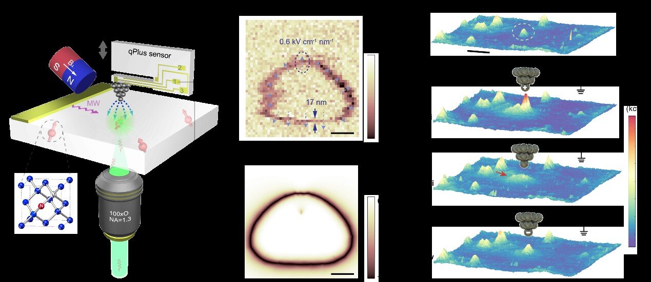
 Figure: (a) Schematic graph showing the NV-based scanning electrometry. (b) and (c): The experimental and simulating electric-field mapping of a sharp metal tip through the single shallow NV. (d) Charge-state control of single NV by the local electric field of tip. Credit: Peking University
A scanning quantum sensing microscope with nanoscale electric-field imaging
Researchers at Peking University have developed a scanning quantum sensing microscope by using a solid-state qubit, Nitrogen-Vacancy (NV) center, as the quantum sensor. They have, for the first time, realized NV-based nanoscale electric-field imaging and […]
Sustainable cities using quantum sensing
In a recent New Civil Engineer article, Professor Paul Jowitt, professor at the Institute of Engineering and Environment at Heriot Watt University, emphasised the important role played by civil engineers in helping to ‘bring a […]
QLM raises £3.1m in seed investment
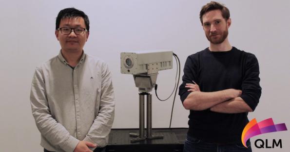
QLM, a quantum-enabled gas sensor startup, in the UK has raised £3.1m (€3.6m) in a seed investment. The company has developed a lidar camera using quantum photon sensor that can detect methane, a key greenhouse gas, […]
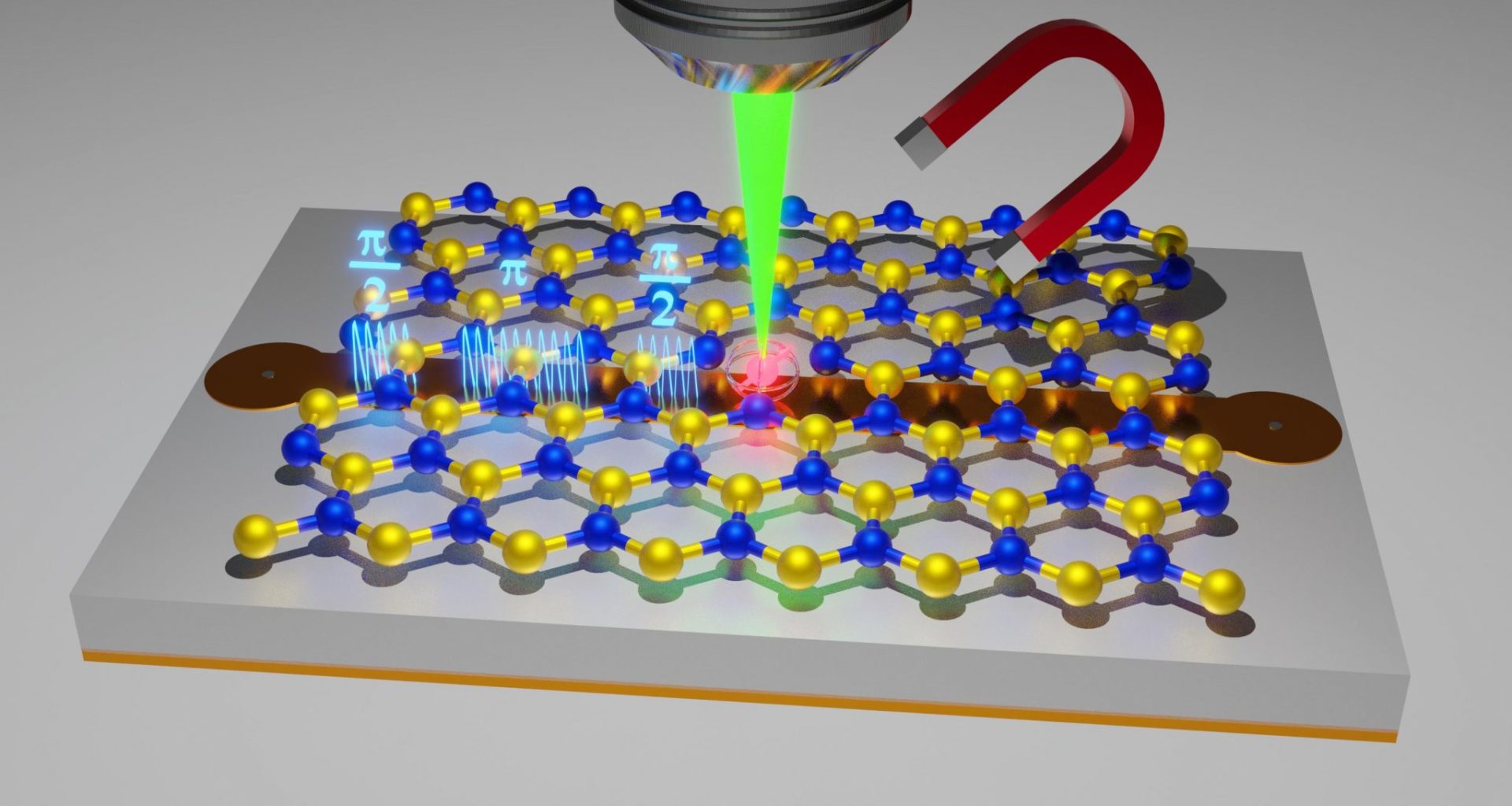
 Schematic representation of the coherent control of a spin defect (red) in an atomic layer of boron nitride. Boron nitride consists of boron (yellow spheres) and nitrogen (blue spheres) and lies on a stripline. The spin defect is excited by a laser and its state is read out via photoluminescence. The qubit can be manipulated both by microwave pulses (light blue) of the stripline and also by a magnetic field. Credit: Andreas Gottscholl / University of Wuerzburg
Quantum Sensing: Spin defects under control
About a year ago, a team from the Institute of Physics at Julius-Maximilians-Universität (JMU) Würzburg in Bavaria, Germany, succeeded in creating spin defects, also known as qubits, in a layered crystal of boron nitride and […]
Governing airspace with quantum-enabled radar
Flying taxis sound improbable but are actually just a short time away from being realised. A recent Economist article highlighted the growing investment being poured into this new vehicle sector across the world, and in […]


