In the new method, two boron nitride (n-BN) layers twisted with respect to each other create an electric field in a molybdenum diselenide semiconductor (MoSe2). A light beam (red) is used to study the properties of the electrons in the semiconductor. Credit: ETH Zurich

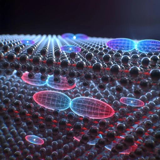
Harnessing Coulomb Interactions in Nanoscale Ferroelectric Moiré Structures

Researchers created a nanoscale ferroelectric moiré pattern using hexagonal boron nitride layers to generate a purely electrostatic potential that enhances Coulomb interactions in transition metal dichalcogenides, enabling optical detection of electron correlations and ordered states while opening pathways to explore exotic quantum phenomena like chiral layer-pseudospin liquids and kinetic magnetism.

The illustration shows the layers of semiconductor crystal stacked together. Electron orbitals within the layers are represented as sitting atop them. The double-lobed orbitals indicate the locations of excited electrons while single ellipsoids show the ground state, where empty spaces called holes are left behind. Although similar orbitals might be expected running front to back, or in and out of the layers, the research team co-led by the University of Regensburg and University of Michigan showed why excited electrons are mainly funneled into one orientation of this orbital. Credit: Brad Baxley, Part to Whole, edited; Copyright: DOI: 10.1038/s41563-025-02120-1

Quantum “Miracle Material” Enables Magnetic Switching

Researchers from the University of Regensburg and the University of Michigan discovered that chromium sulfide bromide functions as a quantum “miracle material” capable of encoding information in multiple forms (charge, light, magnetism, and vibrations) while its unique magnetic properties confine excitons to single layers or lines, significantly extending quantum information longevity and potentially enabling rapid conversion between photon and spin-based quantum information.