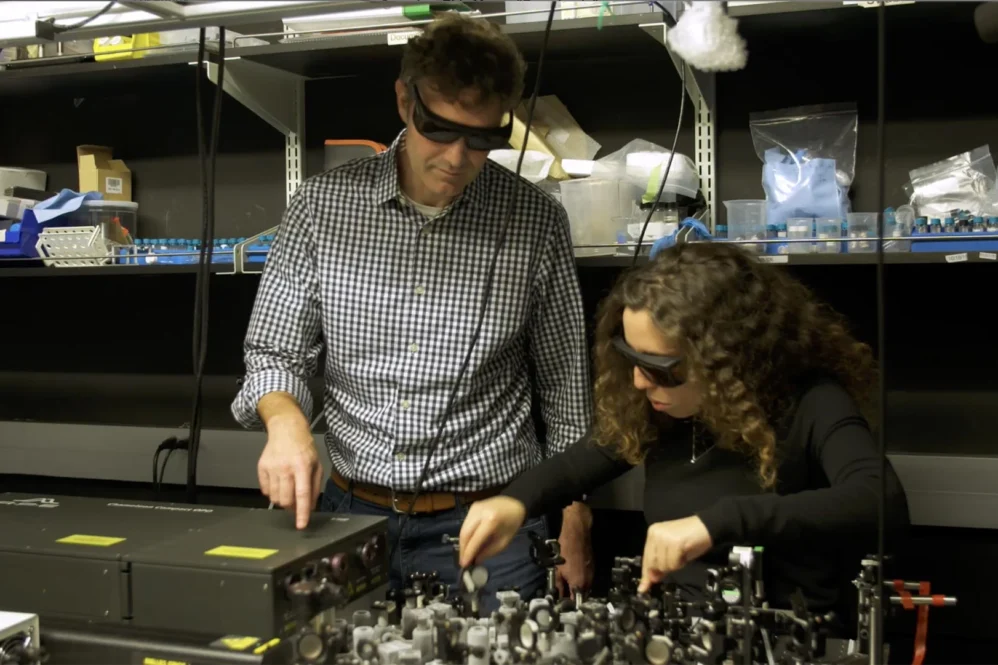
The Columbia Engineering research team, led by P. James Schuck, has achieved a remarkable breakthrough in quantum technology by developing a miniaturized device that generates entangled photon pairs. Their groundbreaking work, published in Nature Photonics on January 13, represents a significant advancement in nonlinear optics and quantum information processing.
The innovation centers on quantum entanglement, a phenomenon Albert Einstein once termed “spooky action at a distance,” where paired photons maintain instantaneous correlation regardless of their physical separation. While this principle has long been understood theoretically, its practical implementation has traditionally required bulky crystal-based systems visible to the naked eye.
The team’s novel approach dramatically reduces the size requirements while improving performance. Their device measures just 3.4 micrometers in thickness and employs an innovative layered structure of molybdenum disulfide, a van der Waals semiconducting transition metal. The construction consists of six crystal layers, each rotated 180 degrees relative to its adjacent layers, creating a precise stack that enables quasi-phase-matching—a technique that manipulates light properties to generate paired photons.
This breakthrough addresses several critical challenges in quantum technology. The device generates photon pairs at telecommunications-compatible wavelengths, marking the first successful implementation of quasi-phase-matching in van der Waals materials for this purpose. The method demonstrates superior efficiency compared to existing approaches and shows remarkably low error rates, making it particularly valuable for practical applications.
The research builds upon the team’s previous work from 2022, where they initially identified molybdenum disulfide’s potential for nonlinear optics. While their earlier efforts were hindered by light wave interference within the material, the current design overcomes this limitation through periodic poling, effectively managing phase matching at microscopic scales.
The implications of this development are far-reaching. The device’s compact size makes it compatible with silicon chip integration, potentially revolutionizing various quantum technology applications. Its energy efficiency and improved technical capabilities could transform quantum computing, telecommunications, and high-precision sensing systems. Professor Schuck envisions immediate applications in satellite-based distribution and mobile phone quantum communication.
Perhaps most significantly, this achievement bridges the gap between macroscopic and microscopic quantum optics, a long-standing goal in the field. The research team believes their work establishes van der Waals materials as fundamental components for next-generation nonlinear and quantum photonic architectures. These materials could potentially replace current bulk and periodically poled crystals in on-chip technologies.
The development represents a crucial step toward scalable, highly efficient quantum devices that can be integrated into existing technological infrastructure. By solving the size and efficiency challenges that have historically limited quantum technology applications, this breakthrough opens new possibilities for practical quantum systems.
This achievement exemplifies how theoretical physics concepts can be transformed into practical engineering solutions. The team’s success in miniaturizing quantum entanglement generation while maintaining or improving performance demonstrates the potential for quantum technology to become more accessible and integrated into everyday applications. Their work suggests a future where quantum technologies could become as commonplace as traditional electronic devices, with implications spanning from secure communications to advanced computing systems.
Reference: “Quasi-phase-matched up- and down-conversion in periodically poled layered semiconductors” by Chiara Trovatello, Carino Ferrante, Birui Yang, Josip Bajo, Benjamin Braun, Zhi Hao Peng, Xinyi Xu, Philipp K. Jenke, Andrew Ye, Milan Delor, D. N. Basov, Jiwoong Park, Philip Walther, Cory R. Dean, Lee A. Rozema, Andrea Marini, Giulio Cerullo and P. James Schuck, 13 January 2025, Nature Photonics. DOI: 10.1038/s41566-024-01602-z


