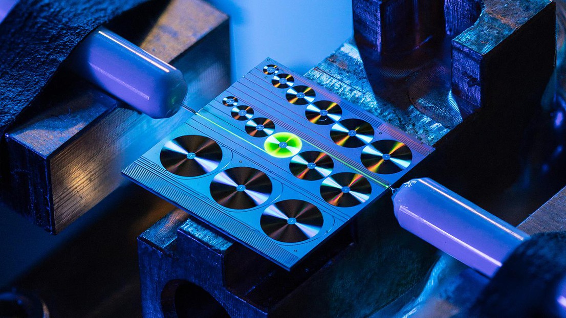
A groundbreaking development in optical memory technology has been announced with the creation of a programmable photonic latch, offering significant improvements in data storage and processing speed for optical systems. This innovation, led by Farshid Ashtiani from Nokia Bell Labs, addresses a crucial gap in optical computing where data storage has traditionally relied on slower electronic memory.
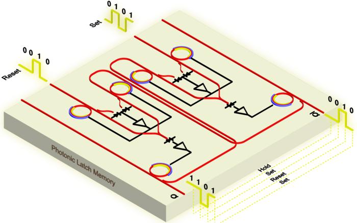
The programmable photonic latch functions similarly to a set-reset latch in electronic systems, storing data in binary states (0 or 1) but using optical signals instead of electrical ones. This advancement is particularly significant because while optical technologies have made substantial progress in communications and computing, data storage has remained predominantly electronic, creating bottlenecks in processing speed and energy efficiency.
The key innovation lies in the development of integrated programmable photonic latches based on optical universal logic gates using silicon photonic micro-ring modulators. These components can be manufactured using existing commercial silicon photonic processes, making the technology both practical and scalable. The system’s design allows multiple memory units to operate independently without interference from optical power loss propagation.
One of the technology’s notable features is its compatibility with wavelength division multiplexing (WDM), enabling multi-bit data storage within a single memory unit. The system achieves impressive response times in the range of tens of picoseconds, surpassing the clock speeds of current advanced digital systems.
The potential applications for this technology are far-reaching, particularly in artificial intelligence and large language models like ChatGPT, which require massive amounts of rapid mathematical operations. The researchers suggest that their memory technology could significantly accelerate these operations by enabling faster data storage and retrieval.
The development addresses several longstanding challenges in optical memory implementation. Previous attempts often relied on bulky, expensive, and energy-intensive setups or required specialized materials not commonly available in commercial silicon photonic processes. The new approach overcomes these limitations by utilizing standard silicon photonic chip fabrication processes, potentially leading to more cost-effective and reliable production.
During testing, the researchers demonstrated the technology’s reliability using a programmable photonic platform. The gates consistently produced the desired outputs even when subjected to random variations, and the latch accurately performed all its functions – set, reset, and hold – despite input power fluctuations.
Looking ahead, the research team has outlined several objectives for making the technology more practical for real-world applications. These include:
- Scaling up the technology to support more memory units
- Developing specialized photonic memory chips
- Increasing on-chip memory density through WDM technology
- Creating an integrated manufacturing process that combines both photonic memory circuits and their electronic control components
While the researchers acknowledge that a commercial optical computer remains a distant goal, this advancement represents a significant step toward that future. The technology’s potential to reduce latency and energy consumption while increasing processing speed could have substantial implications for various applications in AI, sensing, and other computationally intensive fields.
The research has been published in the Optica Publishing Group journal Optics Express, where the proof-of-concept experiment and its results are detailed. This development marks an important milestone in the ongoing evolution of optical computing technology, potentially paving the way for more efficient and powerful computing systems in the future.
Reference: “Programmable photonic latch memory” by F. Ashtiani, 23 January 2025, Optics Express.
DOI: 10.1364/OE.536535


