A significant milestone in silicon photonics has been achieved as an international research consortium has developed the first electrically pumped continuous-wave semiconductor laser specifically designed for silicon integration. The team, comprising scientists from Forschungszentrum Jülich, the University of Stuttgart, IHP, and CEA–Leti, created this groundbreaking device using only group IV elements.
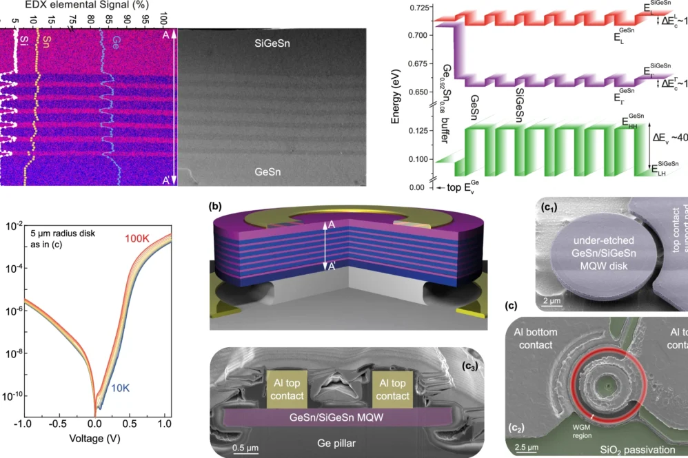
The laser’s innovative design features stacked ultrathin layers of silicon-germanium-tin and germanium-tin grown directly on a silicon wafer, representing a crucial advancement for on-chip integrated photonics. This development addresses a critical gap in silicon photonics technology, as documented in Nature Communications.
The timing of this breakthrough aligns with increasing demands for energy-efficient hardware solutions driven by AI and IoT expansion. While optical data transmission already dominates long-distance communication due to its superior efficiency and data capacity, this technology could extend these benefits to shorter-range applications through photonic integrated circuits (PICs).
The semiconductor industry has made substantial progress in integrating optical components onto silicon chips, successfully developing components such as modulators, photodetectors, and waveguides. However, creating an efficient, electrically pumped light source using only Group IV semiconductors remained an elusive goal. Previous solutions relied on III-V materials, which posed integration challenges and increased manufacturing costs. This new laser, being compatible with standard CMOS technology, represents the final crucial component needed for complete silicon photonic integration.
The technical achievements of this laser are particularly noteworthy. It operates with minimal power requirements, needing only 5 milliamperes at 2 volts – comparable to LED power consumption. This efficiency is achieved through an advanced multi-quantum well structure and ring geometry, allowing stable operation up to 90 Kelvin (-183.15°C). The laser’s fabrication on standard silicon wafers demonstrates its potential for integration with existing manufacturing processes.
While the current version requires cryogenic temperatures to function, the development trajectory of similar technologies suggests room-temperature operation may be achievable in the near future. This optimism is based on the rapid evolution of optically pumped germanium-tin lasers, which progressed from cryogenic to room-temperature operation within just a few years.
The key distinction of this laser lies in its electrical pumping mechanism, which offers superior energy efficiency compared to optically pumped alternatives. Rather than requiring an external light source, it generates laser light directly from electrical current, making it more practical for real-world applications.
This breakthrough represents a significant step toward fully integrated silicon photonics, potentially enabling more efficient and cost-effective optical communication systems for future computing applications. While further optimization is needed to achieve room-temperature operation and reduce the lasing threshold, the foundation has been laid for a new generation of silicon-compatible photonic devices.
Reference: “Continuous-wave electrically pumped multi-quantum-well laser based on group-IV semiconductors” by Lukas Seidel, Teren Liu, Omar Concepción, Bahareh Marzban, Vivien Kiyek, Davide Spirito, Daniel Schwarz, Aimen Benkhelifa, Jörg Schulze, Zoran Ikonic, Jean-Michel Hartmann, Alexei Chelnokov, Jeremy Witzens, Giovanni Capellini, Michael Oehme, Detlev Grützmacher and Dan Buca, 3 December 2024, Nature Communications. DOI: 10.1038/s41467-024-54873-z


