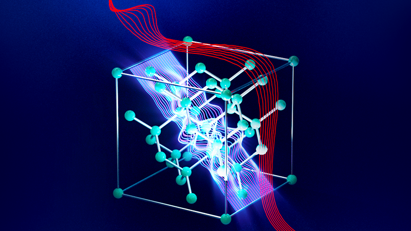
Researchers at Purdue University have made a groundbreaking discovery in the field of light-matter interaction, identifying new waves with picometer-scale spatial variations of electromagnetic fields that can propagate in semiconductors like silicon. This significant advancement, termed “picophotonics,” moves beyond the microscopic realm into the picoscopic regime, where the discrete arrangement of atomic lattices fundamentally alters light’s properties.
The research team, led by Dr. Zubin Jacob, Elmore Associate Professor of Electrical and Computer Engineering and Department of Physics and Astronomy, published their findings in APS Physics Review Applied.
Dr. Jacob explains that while “microscopic” refers to a length scale of a micron (one-millionth of a meter), their work explores light-matter interaction at the picoscopic level—far smaller—revealing surprising properties as light interacts with atomic lattice structures. These findings demonstrate that natural media contain rich light-matter interaction phenomena at the atomistic level, potentially leading to new functional optical devices for quantum technologies.
Light-matter interaction forms the foundation of photonic devices from lasers to detectors. While nanophotonics has advanced our understanding of light flow at the nanometer scale in engineered structures like photonic crystals and metamaterials, these approaches relied on classical theory. The picophotonics breakthrough emerged from a quantum theory of atomistic response in matter, developed by Dr. Jacob along with research scientist Dr. Sathwik Bharadwaj and former post-doc Dr. Todd Van Mechelen.
The team solved a long-standing puzzle regarding the relationship between atomic lattices, their symmetries, and their effects on picoscopic light fields by developing a Maxwell Hamiltonian framework combined with a quantum theory of light-induced material response. This marks a pivotal shift from the classical treatment applied in nanophotonics, emphasizing that quantum behavior of light in materials is key to picophotonic phenomena.
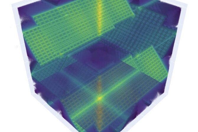
Bharadwaj and colleagues demonstrated that new anomalous waves emerge within the atomic lattice, hidden among traditional electromagnetic waves. These light waves oscillate significantly even within a single fundamental building block of silicon crystal at sub-nanometer scales. The team now aims to apply their theory to quantum and topological materials while experimentally verifying these new waves.
Dr. Jacob’s group has established the picoelectrodynamics theory network, bringing together diverse researchers to explore macroscopic phenomena stemming from microscopic pico-electrodynamic fields inside matter.
Reference: Sathwik Bharadwaj, Todd Van Mechelen, Zubin Jacob. Picophotonics: Anomalous Atomistic Waves in Silicon. Physical Review Applied, 2022; 18 (4) DOI: 10.1103/PhysRevApplied.18.044065


