Quantum Sensing: Spin defects under control

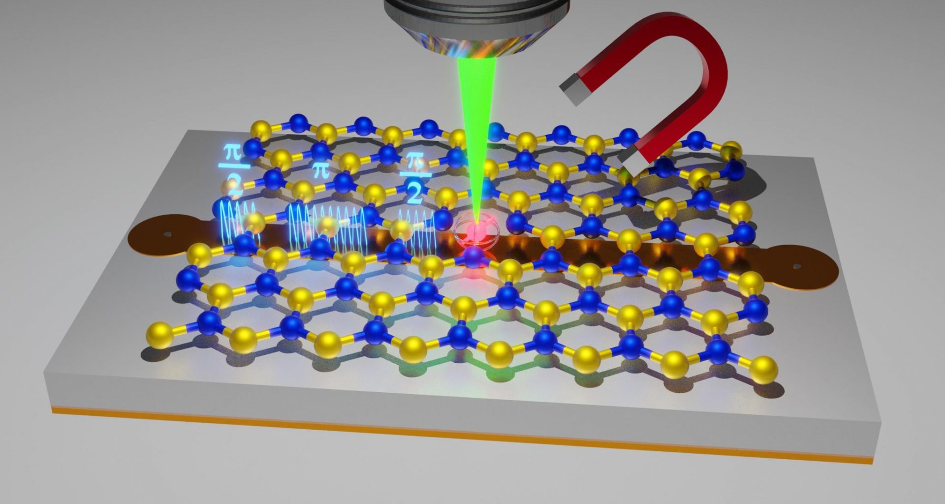
Schematic representation of the coherent control of a spin defect (red) in an atomic layer of boron nitride. Boron nitride consists of boron (yellow spheres) and nitrogen (blue spheres) and lies on a stripline. The spin defect is excited by a laser and its state is read out via photoluminescence. The qubit can be manipulated both by microwave pulses (light blue) of the stripline and also by a magnetic field. Credit: Andreas Gottscholl / University of Wuerzburg

About a year ago, a team from the Institute of Physics at Julius-Maximilians-Universität (JMU) Würzburg in Bavaria, Germany, succeeded in creating spin defects, also known as qubits, in a layered crystal of boron nitride and identifying them experimentally.

Recently, the team succeeded in taking an important next step: the coherent control of such spin defects, and that even at room temperature.
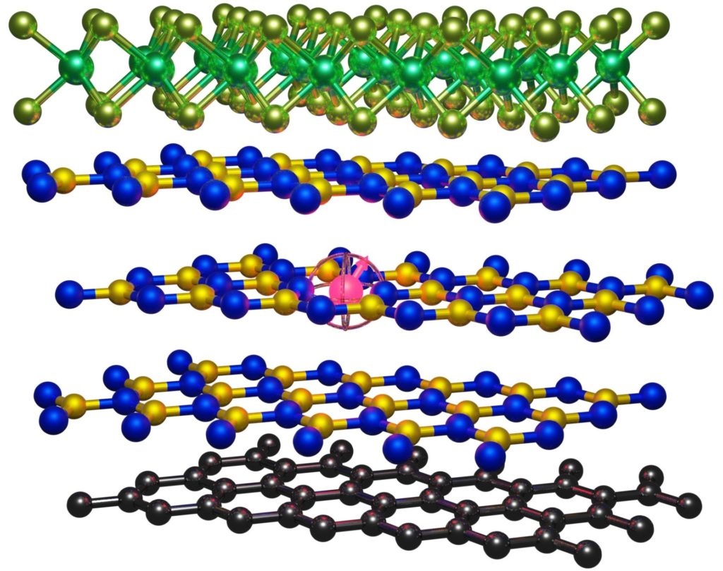
The JMU researchers plan to realize such a stacked structure. It consists of metallic graphene (bottom), insulating boron nitride (middle) and semiconducting molybdenum disulfide (top). The red dot symbolizes the single spin defect in one of the boron nitride layers. The defect can serve as a local probe in the stack. Credit: Andreas Gottscholl / University of Wuerzburg

The contactless manipulation of the “gyroscope” (the spin state) was achieved through the pulsed high-frequency electromagnetic field, the resonant microwaves. The JMU researchers were also able to determine how long the “gyroscope” maintains its new orientation. Strictly speaking, the deflection angle should be seen here as a simplified illustration of the fact that a qubit can assume many different states, not just 0 and 1 like a bit.

What does this have to do with sensor technology? The direct atomic environment in a crystal influences the manipulated spin state and can greatly shorten its coherence time.

The JMU team’s next goal is to realize an artificially stacked two-dimensional crystal made of different materials, including a spin-bearing component. The essential building blocks for the latter are atomically thin boron nitride layers containing optically active defects with an accessible spin state. (SciTechDaily)

The paper has been published in Science Advances.

Read more.

Previous Article

ETH and PSI create a joint Quantum Computing Centre

Next Article

Processing Quantum Signals Carried by Electrical Currents

You might be interested in …

Leave a Reply

Your email address will not be published. Required fields are marked *

This site is protected by reCAPTCHA and the Google Privacy Policy and Terms of Service apply.

The reCAPTCHA verification period has expired. Please reload the page.