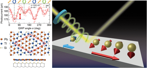
A University of Tokyo research team has achieved a significant breakthrough in spintronic technology by successfully controlling spin-polarized current direction in single-atom thallium-lead alloy layers at room temperature. Led by researchers Ibuki Taniuchi, Ryota Akiyama, Rei Hobara, and Shuji Hasegawa, this discovery fundamentally challenges previous understanding of how ultra-thin materials interact with light, as single-atom layers were traditionally thought to be nearly transparent.
The research, published in ACS Nano, demonstrates the Circular PhotoGalvanic Effect (CPGE) in two-dimensional systems. This phenomenon involves converting light into spin-polarized current, where electron spins align in one direction, thereby controlling current flow based on light polarization. This mechanism mirrors the functionality of conventional diodes but operates at an atomic scale.
The significance of this breakthrough lies in its potential applications for next-generation electronics. As devices continue to shrink, traditional diode manufacturing becomes increasingly challenging. The team’s work with spintronics in ultra-thin systems offers a promising solution by manipulating electron spin rather than conventional charge-based approaches. This could lead to the development of environmentally friendly data storage solutions and ultra-thin, two-dimensional spintronic devices.
To achieve these results, the researchers conducted their experiments in an ultra-high vacuum environment to prevent material oxidation and adsorption, allowing them to observe the material’s true properties. When they exposed the thallium-lead alloys to circular polarized light, they observed controllable changes in both the direction and magnitude of the electrical current. Notably, the electron spin aligned with the current direction due to the unique properties of these thin alloys.
The discovery was partly serendipitous, building upon the team’s previous work with thin alloys that exhibited unusual electronic properties. Looking ahead, the research team, led by Akiyama, plans to optimize the system further by exploring novel two-dimensional thin alloys and investigating the use of lower energy terahertz lasers. This approach aims to narrow the excitation paths that induce CPGE, potentially increasing the efficiency of light-to-spin-polarized current conversion.
This advancement represents a crucial step forward in the field of spintronics, traditionally focused on thicker materials. By successfully demonstrating these effects in two-dimensional systems, the research opens new possibilities for ultra-thin electronic components and data storage solutions. The work underscores the importance of basic research in driving technological innovation and suggests a promising direction for the future of electronic device development.
The findings have significant implications for the future of electronic device miniaturization and efficiency, potentially leading to more sustainable and powerful computing technologies. This breakthrough exemplifies how fundamental research in materials science continues to push the boundaries of what’s possible in electronic device engineering.
Reference: “Surface Circular Photogalvanic Effect in Tl–Pb Monolayer Alloys on Si(111) with Giant Rashba Splitting” by Ibuki Taniuchi, Ryota Akiyama, Rei Hobara and Shuji Hasegawa, 10 January 2025, ACS Nano. DOI: 10.1021/acsnano.4c08742


